Today’s SoC designers are facing the challenge of integrating PCIe 7.0 into new AI chip designs to meet the growing demands of data-intensive applications. The success of first-pass silicon is crucial in achieving the required performance and bandwidth.
The evolution of data center technologies is essential to support the increasing workload and demands of AI, especially with the exponential growth of parameters every four to six months. Current AI models boast trillions of parameters, pushing existing infrastructures to their limits and necessitating more capacity, resources, and faster interconnects.
According to Synergy Research Group, hyperscale data centers globally are expected to double in size over the next six years to accommodate generative AI needs. Standards like PCIe, CXL, Ethernet, and HBM play a crucial role in providing the necessary framework for performance, capacity, bandwidth, and low latency in data transfer within the system.
Efficient interconnects and interfaces are vital for the success of data center chip designs. Designers require high-speed performance with zero latency, the capacity to handle massive data transfers, and access to advanced interface IP that offers bandwidth, power efficiency, and interoperability with the evolving ecosystem.
To meet these demands, data center interconnects must support PCIe 7.0, the latest specification of this critical standard. Integrating IP that supports PCIe 7.0 into a silicon roadmap early is essential, given the lengthy production timeline of today’s chips. Figure 1 illustrates the significance of PCIe 7.0 for interconnect providers and its potential impact on the AI/ML fabric.

Figure 1. PCIe 7.0 offers the bandwidth and load-store capabilities needed to connect multiple accelerators, enabling them to process large, complex AI models effectively.
The next leap in performance
PCIe 7.0 is set to provide the necessary bandwidth for scaling interconnects in hyperscale data centers, offering fast and secure data transfers with up to 512 GB/s bandwidth. This future-proofs data center bandwidth to prevent data bottlenecks.
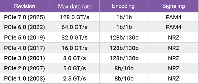
Facilitated by interface IP, high-speed interfaces on processors, accelerators, switches, and more can efficiently move data within the compute fabric, enhancing signaling rates, reducing latency, and ensuring real-time processing for AI algorithms and high-speed data processing in HPC. PCIe 7.0 expands the number of supported lanes and doubles the bandwidth while maintaining backward compatibility with previous generations and enabling scalability for future upgrades. Table 1 outlines the evolution of PCIe through its various versions.

Table 1. Comparison of data rates for PCIe versions.
Maintaining critical interoperability
Interoperability, particularly with mature standards like PCIe, is crucial for a diverse ecosystem of vendors to collaborate effectively, ensuring reliable operation of components and systems. Seamless operation over an extended period is essential when designing high-performance chips to avoid downtime and performance issues.
Prior to system design and IP selection, designers must conduct a thorough evaluation considering the variants, lanes, media, form factors, and reaches of PCIe. Issues like power integrity and signal integrity analysis are vital, especially in designs requiring multiple high-speed lanes and simultaneous switching. Engineers must possess expertise in power and signal integrity to achieve optimal performance.

Figure 2. PCIe’s high-speed digital signals require intense signal-integrity analysis to reach sign-off of first-pass silicon.
Why PCIe 7.0 today?
Deploying tomorrow’s AI clusters with accelerators, switches, network interface cards, etc., simultaneously is crucial for data-intensive operations without bottlenecks. Early access to IP supporting PCIe 7.0 before the standard’s ratification is essential for companies to initiate HPC and AI chip designs early, ensuring the required bandwidth and performance for top-tier chips.


