Photonic integrated circuits (PICs) offer high-speed data transmission, low power consumption, and compact size, making them ideal for integration into edge devices. They are increasingly utilized in signal processing for edge AI and sensor applications.
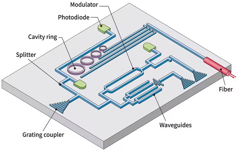
Silicon photonics is a broad technology based on CMOS processing, heterogeneous integration, and advanced optical functionality. Silicon-on-insulator (SOI) plays a crucial role. Some key elements of PICs include (Figure 1):
- Optical waveguides can be made with silicon or silicon nitride, facilitating efficient on-chip optical connectivity.
- Optical ring resonators are fundamental building blocks that can integrate with optical filters, modulators, multiplexers, and frequency comb generators. Specialized designs like Fabry-Pérot resonators and Whispering Gallery Mode resonators cater to specific functions.
- Modulators adjust photonics properties such as phase, polarization, and intensity to enhance PIC performance.
- Photodetectors establish connectivity between the optical and electrical sections of PICs and the external environment.
- Optical coupling elements merge, split, or redistribute optical signals. Grating couplers and edge couplers are common choices, each offering unique advantages.
PICs in edge AI
PICs enhance lower latencies for applications like LIDAR in autonomous vehicles and robots, enabling safer navigation. They consume significantly less energy than conventional ICs, crucial for energy-constrained edge devices.
Processing data on the edge device reduces the reliance on cloud connectivity, further saving energy. Minimizing wireless connectivity enhances the resilience of edge devices.
PICs in advanced sensors
PICs find applications in highly sensitive and compact sensors for edge use. Combined with edge AI, they can execute real-time object and facial recognition, along with other intricate image processing functions, directly on the sensor chip.
PIC sensors are employed in environmental monitors to detect pollutants and measure air or water quality. They also play a role in food processing to determine parameters like ripeness and nutrient content.
PIC lab on a chip
PIC sensors enable swift diagnostics of medical and environmental conditions in the field, eliminating the necessity for remote laboratories. They often offer higher sensitivities and superior outcomes. Some PIC sensors can reliably detect attomolar concentrations of substances dissolved in a solution.
Integrated optical sensors for these applications typically use silicon nitride (SiN) for fabrication. SiN waveguides exhibit good sensitivity across the visible to near-infrared range and can be bent with a small radius, enabling long sensors to occupy minimal space on a PIC surface.
Certain sensor designs feature a coating that alters its refractive index upon encountering target molecules. Changes in the refractive index are detected using photonic transducers and connected to the lab-on-a-chip via optical waveguides (Figure 2).
Figure 2. Lab-on-a-chip biosensors like this, based on PICs, can provide real-time data for medical diagnostics. (Image: Aventier)
Other photonics platforms
PICs are versatile and can be crafted with materials beyond silicon and silicon nitride. Many PICs incorporate silica (SiO2) for functionalities like planar optical waveguides.

Figure 3. This tunable laser system utilizes hybrid integration, combining a low-loss SiN PIC with a high-performance active gain InP PIC. (Image: PhotonDelta)
Lithium Niobate (LiNbO3) is employed for producing low-loss modulators due to its optical properties. Lithium Niobate on Insulator (LNOI) technology is in development for future PIC designs.
Heterogeneous or hybrid integration of PIC technologies can optimize system cost and performance simultaneously. For instance, a tunable laser system combines a low-loss SiN PIC with a high-performance active gain Indium Phosphide (InP) PIC (Figure 3).
Summary
PICs are increasingly utilized in various edge applications, including data processing and sensor integration. They reduce energy consumption, enhance processing capabilities, and can be implemented on single chips or through heterogeneous integration, incorporating multiple semiconductors and sensor technologies.
References
Designing a Photonic Integrated Circuit: Best Practices for Simulation & Layout, SimuTech
Exploring Photonic Integrated Circuits and Optical ICs, Avantier
High-performance analog signal processing with photonic integrated circuits, Light Science and Applications
Introduction to Silicon Photonics, Santec
Photonic Computing Takes a Step Toward Fruition, APS Physics
Photonic Integrated Circuit (PIC), AyarLabs
What is a Photonic Integrated Circuit?, Ansys
What is a Photonic Integrated Circuit?, PhotonDelta
What is Integrated Photonics?, AIM Photonics
EEWorld Online related content
How are single photon sensors used in quantum computing?
Accelerating high-performance AI workloads with photonic chips
What’s the difference between a VCSEL and PCSEL?
How can in-package optical interconnects enhance chiplet generative AI performance?
How does UCIe on chiplets enable optical interconnects in data centers?
Filed Under: FAQ, Featured