
Metalenses are innovative optical lenses that are flat and lightweight, replacing traditional bulky curved lenses with a specially designed surface featuring nanoscale structure. They can enhance optical system performance and significantly reduce system size and weight.
A metalens is a single thin, flat structure that can often deliver the same performance as multiple conventional optical components.
It consists of multiple waveguides in the shape of pillars, approximately 600 nm long, made from various dielectric materials and arranged side by side (Figure 1). The flat planar structure allows all wavelengths of light to pass through a metalens simultaneously, eliminating chromatic aberrations and making them achromatic.

While the basic design is achromatic, metalenses can be produced with tunable dispersions and can manipulate how specific wavelengths (colors) of light are dispersed. Traditional lens designs have fixed dispersions.
Fabricating metalenses
For near-infrared applications, metalenses are often fabricated using a silicon-on-glass substrate. Metalenses for visible wavelengths are primarily made from dielectric materials such as titanium dioxide (TiO2), gallium nitride (GaN), and silicon nitride (SiN), which have high refractive indices in the visible spectrum.
Metasurfaces can be mass-produced using mature CMOS fabrication nodes readily available in foundries, enabling the wafer-scale integration of metalens-based optical systems. A typical metalens consists of millions of subwavelength unit-cells, also known as meta-atoms.
These meta-atoms can control the phase of light in a highly precise manner, creating the same phase profile as a classic curved lens structure (Figure 2). Meta-atoms typically measure tens of nanometers. For instance, metalens designs with SiN nano-posts on a fused silica substrate, featuring widths between 100 nm and 310 nm, can be used for applications in the visible to near-infrared (NIR) wavelength range.

Figure 2. Metalenses (right) can focus light just like a conventional optical element (left). (Image: Synopsys)
Numerical apertures are important
Metalenses have superior numerical apertures (NAs) compared to traditional lens designs. The NA of a lens describes its ability to collect light and resolve small details, critical for lens performance, especially in microscopy.
A higher NA indicates better performance, allowing a lens to gather more light and produce a brighter image. It also signifies the ability to distinguish between closely spaced objects and deliver highly detailed images.
To emphasize the importance of high NA, a study analyzed fluorescence correlation spectroscopy (FCS) of Alexa Fluor 647, a bright far-red fluorescent dye commonly used in biological and chemical research for labeling molecules.
Comparing performance using a metalens with an NA of 0.6, two single-element aspheric lenses with NAs of 0.18 and 0.54, and a series of achromatic lenses with NAs from 0.15 to 1.2 (Figure 3), the aspheric lenses failed to detect the dye samples, while the metalens performed comparably to the much larger achromatic objective lenses.
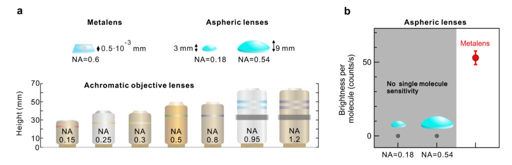
Figure 3. A metalens with an NA of 0.6 is much smaller than aspheric or achromatic lenses (a), and the relatively small aspheric lenses had a brightness of zero and were not able to detect the dye molecules (b). (Image: nature communications)
Metalenses and VCSELs
The compact sizes and high performance of metalenses are being combined with vertical cavity surface-emitting lasers (VCSELs) to create more compact and versatile light sources. VCSELs are semiconductor lasers that emit light vertically from the surface of a wafer.
In VCSEL-illuminated applications, a single metalens can perform functions that would otherwise require several refractive surfaces, leading to ultra-compact and simpler-to-assemble modules. When combined with VCSELs, metalenses can be fabricated using a gallium arsenide (GaAs) film.
Some capabilities of a metalens and VCSEL system include:
- Shaping VCSEL beams with metalenses to create desired illumination patterns, such as dot arrays for facial recognition and simultaneous localization and mapping (SLAM), and line patterns for autonomous mobile robot (AMR) obstacle avoidance.
- Reducing the divergence angle of light emitted by a VCSEL, collimating it, and enhancing its effectiveness in applications like LIDAR and endoscopy.
- Improving laser beam uniformity and contrast compared to conventional beam shaping techniques.
Summary
A metalens is a planar structure comprised of thousands or millions of pillar-shaped optical waveguides. They can fulfill the same functions as conventional optical elements while offering increased flexibility. Despite their small size, they possess high NAs essential for bright and detailed images. Fabricated using conventional CMOS processes, metalenses can be seamlessly integrated with VCSELs, combining the strengths of both technologies to deliver unique optical system capabilities.
References
Concept of a Convex on-Chip Metalens as a Miniature Sensor of Fluorescence of Single Molecules, Methods of Physical Research
Dual-wavelength metalens enables Epi-fluorescence detection from single molecules, nature communications
Flat Lenses Made of Nanostructures Transform Tiny Cameras and Projectors, IEEE Spectrum
How metalenses are reshaping the future of optics, Radiant Vision Systems
Meta Optical Elements (MOE), NIL Technology
What are Meta-optics, Metalenz
What Is a Metalens?, Synopsys
What is a Metalens and How Do They Work?, Ansys
EEWorld related content
How does multi-sensor calibration work in autonomous vehicles?
What is hyperspectral imaging?
What are the defense applications of electro-optical sensors?
What determines the connectivity bandwidth needed in a machine vision system?
How are VCSELs used in biomedical sensors?
Filed Under: Uncategorized